AD574A 12-Bit A/D Converter
The weather station project will measure Environmental Temperature using Temperature Transducer and then its measured results will need to read by microcontroller 8051, here will need an Analog to Digital Converter (ADC). The ADC will convert the measured temperature signal from analog to digital signal readable by Microcontroller. In this project we are going to use AD574A , 12 bit ADC. Lets explores the features of this ADC.
FEATURES OF ADC:
- It is an ADC having 12-Bit analog to digital conversion resolution with provision of user defined Reference voltages and Clock signal
- This ADC can be easily interface with 8 or 16 Bit Microprocessor, here in our case the 8051 family microcontroller is 8 Bit microcontroller, so we can use AD574A with 8051.
- The excellent Linearity over Temperature which is around 08C to +70C
- Very good conversion time like around 35msec for full conversion.
The ADC : AD574A is a 12-bit successive approximation analog to digital converter. The AD574A have Three state output buffer circuit, which facilitates the direct interface to an 8-bit microcontroller like 8051 family. The voltage reference and clock are included on-chip it means that we don't need to build any circuit for voltage reference and clock while using this ADC. The Multiple mode operation of ADC like the three state output buffers connects directly to the data bus while the read and convert commands are taken from the control bus. The 12 bits of output data can be read either as one 12-bit word or as two 8-bit bytes (one with 8 data bits, the other with 4 data bits and 4 trailing zeros). The AD574A contains on-chip logic to provide conversion initiation and data read operations from signals commonly available in microcontroller based systems.
The control
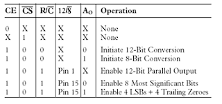
signals like chip enable: CE, chip select: CS, and Read Control: R/C PINs of ADC are the basic control bus which are used to control the operation of the converter. How we will know that the conversion is ready or read operation is ready, its all on the state of R/Ĉ pin. when R/Ĉ = 1 read operation is ready and when it is equal to logic zero then it means that the conversion is in progress.
The register control inputs named as AO will determine the length and data format like 12 or 8 bit conversion . The AO line is normally tied with the least significant address bit of the bus. Now we will see, If a conversion is started with AO at logic zero or low, a full 12 bit conversion cycle will be available to read. Now there is an other case when AO is high during a convert start, then the shorter 8-bit conversion cycle is resulted. In addition to that during data read operations, AO will determine whether the three state buffers containing the 8 MSBs of the conversion result (AO = 0) or the 4 LSBs (AO = 1) are available there.
Therefore we can say that the 12 or 8 pin
determines whether the output data is to be organized as two 8 bit words or a single 12 bit word corresponding to the logic level on this pin. It is very noticeable thing that this very important control pin is not TTL logic compatible Pin rather it is required to be hard wired to either VLOGIC or DIGITAL
COMMON of there analog to digital converter AD574A. Below is the truth table of the ADC for better understanding of above discussion along with the role of other control pins of ADC used during the conversion process.
 |
| ADC: AD574A Truth Table Describing the conversion operation |
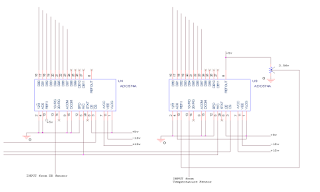
In the 8bit conversion mode, the ADC is byte addressed when AO is at logic high and output port contains the 4 LSBs conversion results followed by four trailing bits containing zeroes. This data organization of ADC allows the data lines to be overlapped which is more suitable for direct interface to 8bit buses. In this way the need for external three-state buffers is not significant. ADC: AD574A as an essential Electronics Component of Weather System. To convert the analog signal to digital signal which is readable or understandable by microcontroller world , the use of ADC is really needed. The 12 bit conversion on ADC is initiated in both of the configurations discussed earlier. The control signals required for initiating the conversion process and then to complete the read operation are of course provided by microcontroller in pour case 8051. The tri-state conditions on output buffer can be used by CS (Chip Select pin which is active on logic low) again it is control signal. All the data that has been read by microcontroller is of 8-bit bus compatible interfacing because this requirement is imposed by the data bus size of the microcontroller 8051. The voltage levels are efficiently and accurately chooses to converted the results in proper digital format. In this project this we have used this ADC twice, one for temperature signal conversion and second for conversion of wind direction signal, so the reference voltage levels for both are ADC are not same rather the ADC reference voltages are set according to need as described below:
- In the case of temperature sensor we use 2.56V as reference voltage to ADC.
- In the direction measurement we will use 5V at the reference Input.
 |
| ADC Interface with sensor and Microcontroller in weather station |
TEMPRATURE SENSOR:LM35
Configuration of LM35 In Microcontroller Based Weather Station:
 |
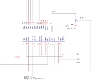
| LM35 interface with AD574A microcontroller 8051 in weather Station |
As the output voltage at nominal room temperature is approximately 0.25V for 25°C and rise up to 1.56V corresponding to 150°C. It reflects that our measurement range of signal will be less than 02V, So we decided to get better results from ADC, the reference voltage should be 2.56V at the reference input(REF/I), so ADC pick the variation only from 0-2.56V.


No comments:
Post a Comment
Please ask if you have any question regarding the programming of MCU, or have any problem in development of your electronics project. microcontroller51.blogspot.com